KiCad 9.0.1 has been released, marking a significant update to this cross-platform, open-source suite for electronics design automation. KiCad excels in managing both schematic capture and printed circuit board (PCB) layout, supporting outputs like Gerber files and IPC-2581, which makes it an invaluable tool for a wide range of design applications.
What is KiCad?
KiCad is a comprehensive integrated workflow solution designed for electronic design, enabling users to create schematic diagrams and PCBs efficiently. This seamless integration ensures consistency across the design process, reducing errors and facilitating a smoother transition from concept to production.
Key Features of KiCad:
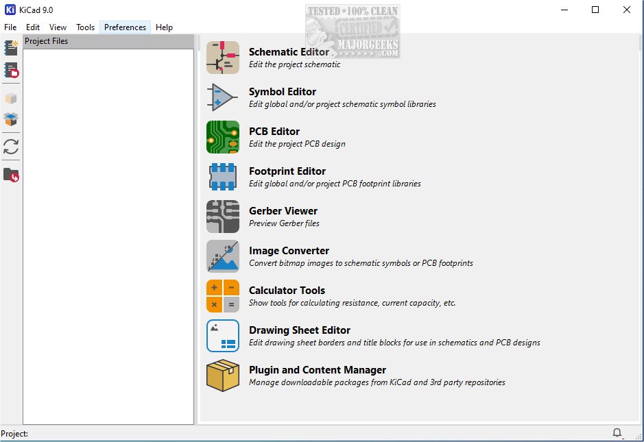
With KiCad, users can create and edit electrical schematics, which are crucial for visualizing the connections and components within electronic circuits. These schematics serve as the foundation for planning the layout of electronic projects. The software provides an extensive suite of layout tools that allow for easy placement of components like resistors, capacitors, and integrated circuits on a virtual board. Furthermore, KiCad offers advanced routing capabilities, enabling users to connect components with traces that closely mimic real-life electrical pathways.
KiCad also includes tools for adjusting parameters such as trace width and clearance, which are vital for ensuring the electrical performance and manufacturability of the final PCB. Once the design is complete, KiCad can generate various manufacturing files, including Gerber files and Bill of Materials (BOM), critical for the production process.
Utilities and Enhancements:
Beyond its primary design functions, KiCad is equipped with a range of utilities that enhance the overall design experience. It features a PCB calculator for determining essential design parameters like trace width, current capacity, and voltage drop. Additionally, a built-in Gerber viewer allows users to inspect their manufacturing files to ensure compliance with fabrication requirements.
KiCad also integrates a SPICE simulator, enabling engineers to perform in-depth circuit analysis. This feature permits users to simulate and validate their designs under various conditions, ensuring reliability and performance before physical prototyping.
Conclusion:
KiCad stands out as a robust platform that caters to both hobbyists and professional engineers, thanks to its powerful features and user-friendly interface. It promotes creativity and innovation in PCB design and electronic circuit development. For those looking to leverage KiCad for their projects, it's highly recommended to consult the provided documentation to get started effectively.
Future Prospects:
As KiCad continues to evolve, future updates may focus on enhancing user experience further, expanding library components, and integrating more simulation capabilities. The community-driven nature of KiCad ensures that user feedback will play a crucial role in shaping the software's development, making it an exciting tool to watch in the electronics design landscape
What is KiCad?
KiCad is a comprehensive integrated workflow solution designed for electronic design, enabling users to create schematic diagrams and PCBs efficiently. This seamless integration ensures consistency across the design process, reducing errors and facilitating a smoother transition from concept to production.
Key Features of KiCad:
With KiCad, users can create and edit electrical schematics, which are crucial for visualizing the connections and components within electronic circuits. These schematics serve as the foundation for planning the layout of electronic projects. The software provides an extensive suite of layout tools that allow for easy placement of components like resistors, capacitors, and integrated circuits on a virtual board. Furthermore, KiCad offers advanced routing capabilities, enabling users to connect components with traces that closely mimic real-life electrical pathways.
KiCad also includes tools for adjusting parameters such as trace width and clearance, which are vital for ensuring the electrical performance and manufacturability of the final PCB. Once the design is complete, KiCad can generate various manufacturing files, including Gerber files and Bill of Materials (BOM), critical for the production process.
Utilities and Enhancements:
Beyond its primary design functions, KiCad is equipped with a range of utilities that enhance the overall design experience. It features a PCB calculator for determining essential design parameters like trace width, current capacity, and voltage drop. Additionally, a built-in Gerber viewer allows users to inspect their manufacturing files to ensure compliance with fabrication requirements.
KiCad also integrates a SPICE simulator, enabling engineers to perform in-depth circuit analysis. This feature permits users to simulate and validate their designs under various conditions, ensuring reliability and performance before physical prototyping.
Conclusion:
KiCad stands out as a robust platform that caters to both hobbyists and professional engineers, thanks to its powerful features and user-friendly interface. It promotes creativity and innovation in PCB design and electronic circuit development. For those looking to leverage KiCad for their projects, it's highly recommended to consult the provided documentation to get started effectively.
Future Prospects:
As KiCad continues to evolve, future updates may focus on enhancing user experience further, expanding library components, and integrating more simulation capabilities. The community-driven nature of KiCad ensures that user feedback will play a crucial role in shaping the software's development, making it an exciting tool to watch in the electronics design landscape
KiCad 9.0.1 released
KiCad: A cross-platform, Open Source suite for electronics design automation that effectively manages schematic capture and PCB (printed circuit board) layout.